100µm to 1.0µm Pitch Finder Grids
January 20, 20161µm Pitch Silicon FINDER GRID
Features
- 525µm ± 20µm thick Boron-doped ultra-flat silicon substrate with resistivity of 5-10ohm-cm and <100> orientation
- Edge fiducial markers for grid position finding
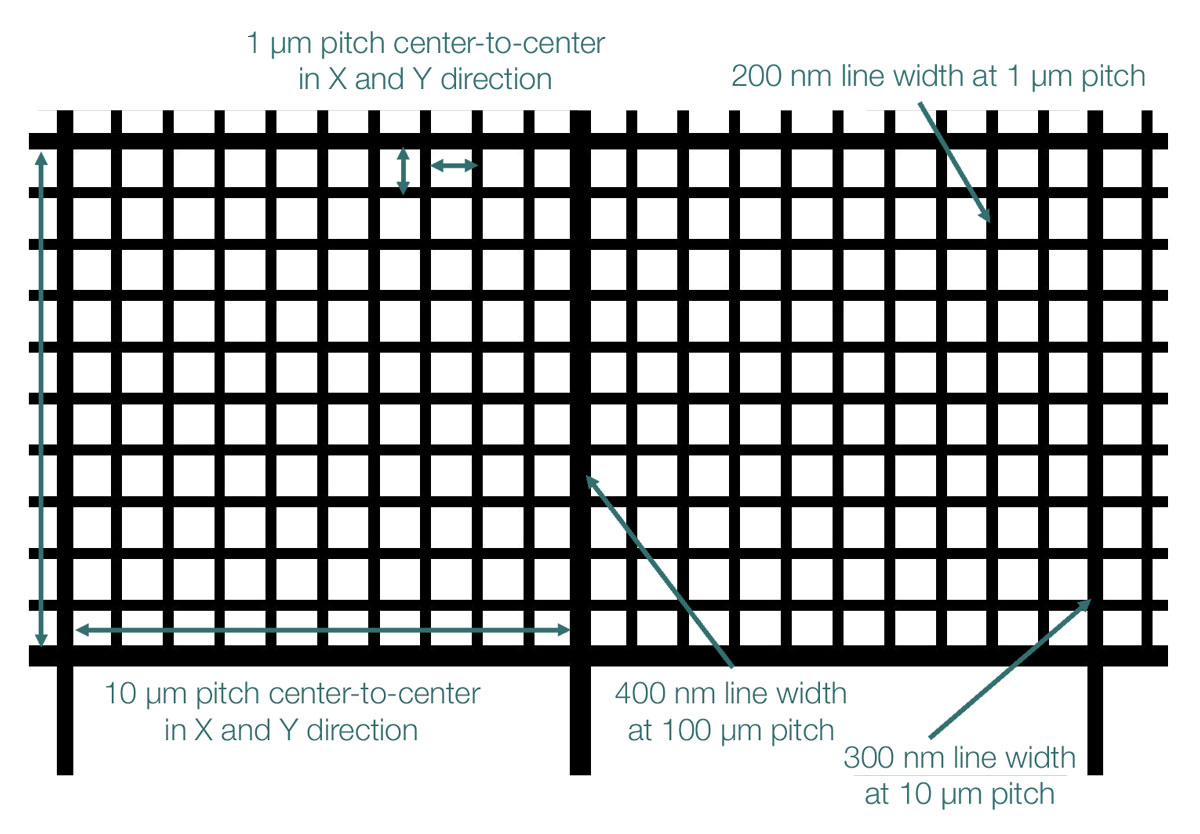
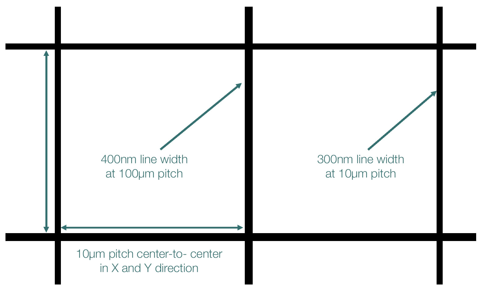
- Pitch of 1µm ± 0.025µm, 10µm ± 0.025µm and 100µm ± 0.25µm with perpendicularity better than 0.01º
- Line width of 200nm ± 10nm for 1µm pitch lines, 300nm ± 15nm for 10µm pitch lines and 400nm ± 20nm for 100µm pitch lines
- 300nm ± 30nm deep etched lines
Whole die layout
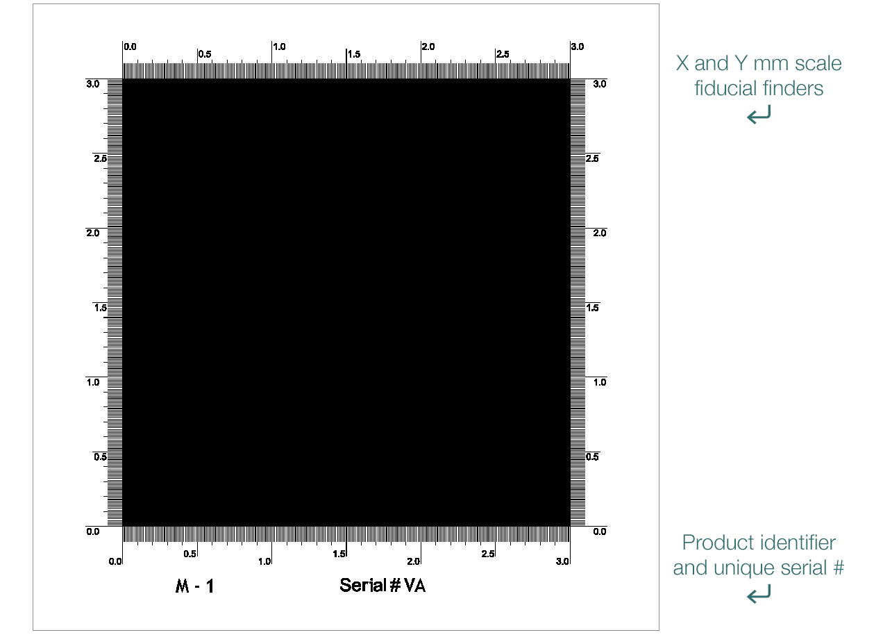
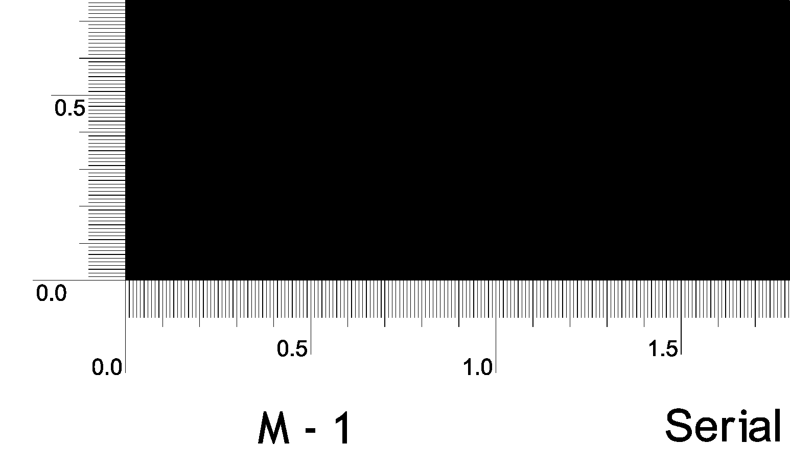
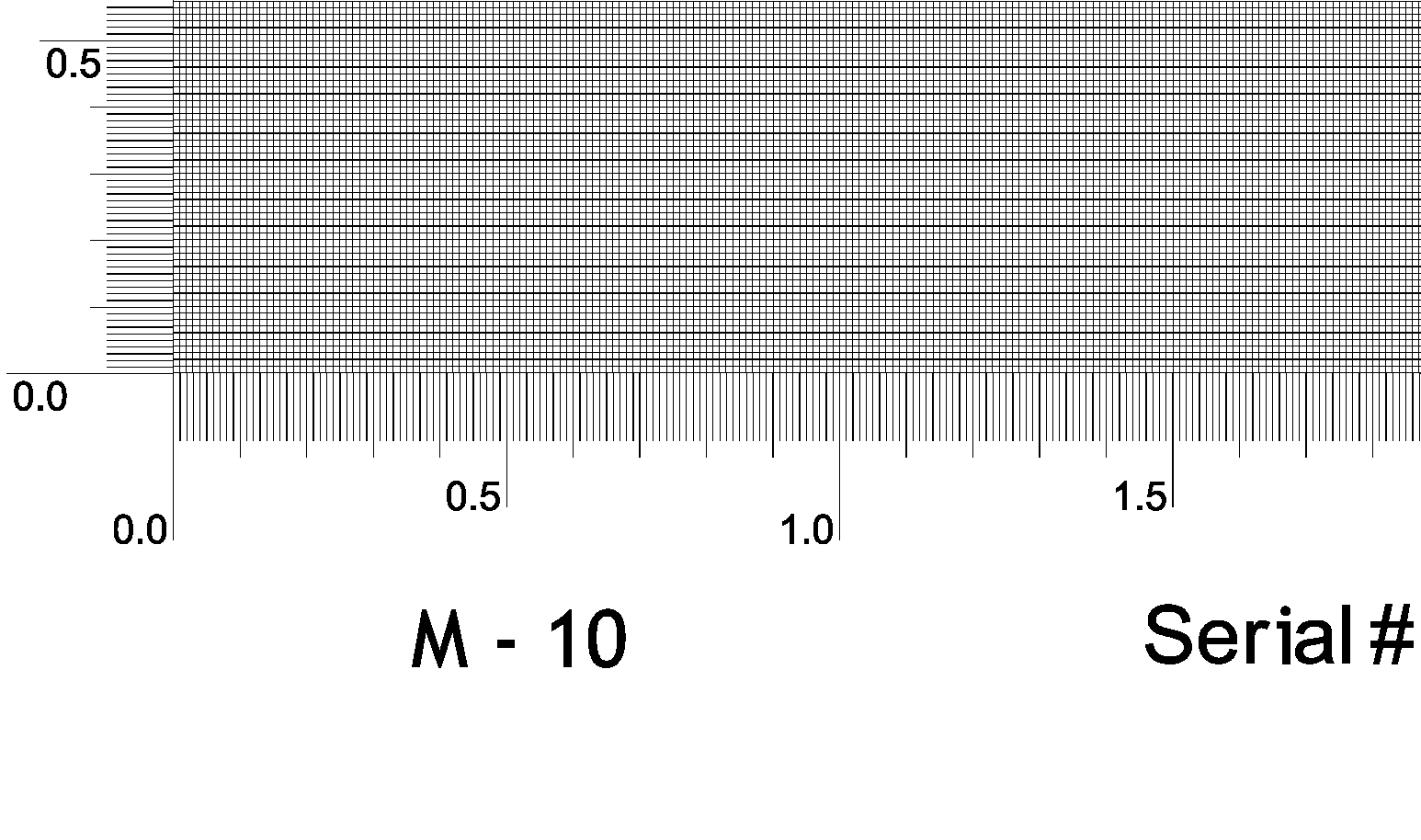
Close-up of major (1.0 and 0.5mm) and minor (0.1mm) fiducial marks
Close-up of minor (100 and 10µm) fiducial marks

Close-up of minor (10µm) fiducial marks and mesh with 1µm pitch

Enlarged view of mesh pattern
10µm Pitch Silicon Calibration Specimen
Features
- 525µm ± 20µm thick Boron-doped ultra-flat silicon substrate with resistivity of 5-10ohm-cm and <100> orientation
- Edge fiducial markers for grid position finding
- Pitch of 10µm ± 0.025µm and 100µm ± 0.25µm with perpendicularity better than 0.01º
- Line width of 300nm ± 15nm for 10µm pitch lines and 400nm ± 20nm for 100µm pitch lines
- 300nm ± 30nm deep etched lines
Whole die layout

Close-up of major (1.0 and 0.5mm) and minor (0.1mm) fiducial marks
Close-up of minor (100 and 10µm) fiducial marks

Close-up of 10µm fiducial lines

Enlarged view of mesh pattern
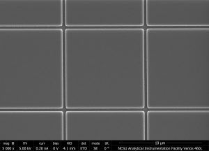
Example SEM Image of 1 micrometer finder grid
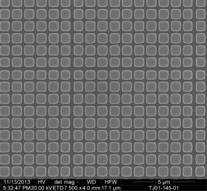
Example SEM Image of 10 micrometer finder grid